
 Photo: Anna-Lena Lundqvist
 Professor Faupel researches and teaches at Kiel University. He has led the Chair for Multicomponent Materials since 1994. His research is focused, amongst others, on functional multicomponent nanomaterials and metal-polymer interfaces. Professor Faupel has already supervised and coordinated NINa since 2005.
 Dr. Fredrik Hörstedt is Vice President for utilisation, industry collaboration and sustainable development at Chalmers University of Technology. He is responsible for Chalmers innovation ecosystem and holds the overall responsibility for Chalmers’ interfaces with business, RTOs, public authorities and politics. He is a board member of the European Innovation Council and an advisor to the Swedish Government on research, innovation and digitalisation.
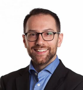
 Jonas Bylander leads a research team focused on developing quantum computers and applying them to computational “use cases” – hard problems that can’t be solved on conventional computers. Jonas has a PhD in Physics from Chalmers. After graduate school he worked as a researcher at MIT for five years, prior to taking up a faculty position back at Chalmers, in 2013. He is currently head of the Quantum Technology Laboratory and a principal investigator in the European Flagship program on Quantum Technology and in the Wallenberg Center for Quantum Technology, WACQT, an initiative aimed to bring Swedish academia and industry to the forefront of quantum technology.
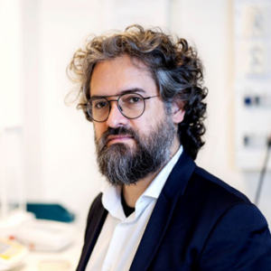 Giovanni Volpe is Professor at the Physics Department at the University of Gothenburg (Gothenburg, Sweden), where he has been leading the Soft Matter Lab since 2016. He has established a strong research group of 18 people (3 postdocs, 12 PhD students, 3 Master students, http://www.softmatterlab.org ) with an externally-funded, ambitious and interdisciplinary research program that combines soft condensed matter, optical manipulation, nanotechnology, and machine learning. He has attracted external funding exceeding 6M €, including several national and European grants such as the ERC-StG ComplexSwimmers (2016-2021) and the ERC-CoG MAPEI (2021-2026). He is a co-funder of the startup companies Lucerio Bio and IFLAI.
 Eva Olsson is a Professor of Experimental Physics at Chalmers University of Technology and a member of the Royal Swedish Academy of Sciences. Her research Division involves advanced imaging and spectroscopic methods of high-resolution electron microscopy for site specific correlation between material structure and properties. Of particular interest is the fundamental understanding of transport mechanisms of charges and matter. The aim is to enable the design of new materials and structures with tailored properties for energy, quantum and health technology.
 Seyed Hosseini, PhD, works as senior researcher at the Research Institutes of Sweden (RISE AB) in the field of additive and subtractive manufacturing processes. Seyed is also working as guest researcher at the Department of Industrial and Materials Science. He focuses primarily of how the materials are affected by the manufacturing processes and potentially how the material or the microstructure could be optimized to improve the product performances. By combining different characterization tools like XRD, SEM, TEM and APT with thermodynamic and kinetic simulations Seyed has during his research in the field of metal cutting developed a phenomenological model describing the microstructural evolution in the hard-turning process. Currently, Seyed is working on the up-scaling of research results in the field of metal cutting into industrial benefit to push for improved product performances and reduced CO2-footprint.
U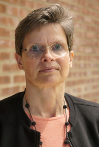 ta Klement is Professor at the Department of Industrial and Materials Science. She heads the Division of Materials and Manufacture and leads the Surface and Microstructure Characterization research group. She works dedicatedly with materials characterization and uses electron microscopy (SEM, TEM) in combination with all necessary complementary techniques to examine the structure-property relationship of engineering materials such as machined surfaces and electrodeposited, thermal sprayed, and additive manufactured materials. Currently, focus is on the development of multifunctional graphene-containing engineering materials with the aim of combining fundamental studies with industrial applications.
 Alexandre Dmitriev obtained his PhD in Physics 2000-2003 on low-dimensional supramolecular systems with metal-organic coordination at Max-Planck-Institute for Solid State Research (Stuttgart, Germany) and EPFL (Lausanne, Switzerland). From mid-2004 – at Chalmers University of Technology (Gothenburg, Sweden), first as EU Marie Curie Fellow, and later as Swedish Research Council Assistant professor, currently – Full Professor at the University of Gothenburg. Visiting professor at Stanford (USA) in 2016-2017 and 2018. Holder of the Swedish Foundation for Strategic Research Future Research Leader and Strategic Research Expedition awards (2010, 2019). Chair (2010-2012) of one of formerly largest European research network in plasmonics (COST Plasmonics), Fellow of the Mobility for Regional Excellence of the Västra Götaland Region, Erskine Visiting Fellow at the University of Canterbury (New Zealand). Research and innovation focus on physics and chemistry of light-matter interactions at the nanoscale.
 Samuel Lara-Avila is Associate Research Professor at the Quantum Device Physics Laboratory, Chalmers University of Technology (Sweden). He specializes on the development, fabrication and study of electron transport properties of low-dimensional systems as well as their use in practical electronics. His work has been recognized with the 2014 International Union of Pure and Applied Physics (IUPAP) Young Scientist Prize in Fundamental Metrology, in recognition of “outstanding contribution to the understanding of quantum electrical transport in epitaxial graphene, leading to the development of a novel quantum Hall resistance standard”. His current work includes interaction between terahertz radiation and charge carriers in graphene, and the development of new 2D materials. He serves as Board Member in the Swedish Physical Society-condensed matter and nano physics, Visiting Scientist at National Physical Laboratory (UK), and Board member at Graphensic AB. Since 2021 he is also Director of the Vinnova competence center 2D-TECH, and the Graphene Center at Chalmers.
 Martin Andersson is Professor and Deputy Head of Department of Chemistry and Chemical Engineering at Chalmers University of Technology. His research interests are in material science and surface chemistry with focus on formation of nanomaterials towards biological applications scientific papers. towards biological applications. In addition to research, Martin is interested in entrepreneurship and is the co-founder of Promimic AB, Amferia AB, Aquammodate AB and Vitroprobe Analytics AB.
Professor Lars Nyborg leads a research group on Powder Metallurgy and Additive Manufacturing and focuses current research on materials development in additive manufacturing (AM) and sintering of powder-based materials. The former research line is connected to the research area novel AM material within the competence centre for additive manufacturing – metals (CAM2). One approach is the nanotech design of powder chemistry and addition of nanoscale particles tune the as-fabricated microstructures in laser powder bed fusion. Another approach is the application of nanoparticles as sintering aid in ferrous powder sintering. The research is run in close co-operation with industry, national co-operation via a framework grant from Foundation for Swedish Foundation for Strategic Research and international co-operation with for example Polytech Torino, Polytech Milano and CSEM within EU-projects.
 Adjunct Professor Karin Frisk focuses current research on development of powder materials for additive manufacturing and surface coating applications, within CAM2 and at Höganäs AB. Computational alloy design based on microstructure predictions, with goal to provide new alloy compositions that are tailored for rapid solidification of relevance for these applications. The modeling is applied to increase the pace of development of new powder alloy compositions, and to increase our understanding of the coupling of microstructure to properties.
Alexandre Dmitriev obtained his PhD in Physics 2000-2003 on low-dimensional supramolecular systems with metal-organic coordination at Max-Planck-Institute for Solid State Research (Stuttgart, Germany) and EPFL (Lausanne, Switzerland). From mid-2004 – at Chalmers University of Technology (Gothenburg, Sweden), first as EU Marie Curie Fellow, and later as Swedish Research Council Assistant professor, currently – Full Professor at the University of Gothenburg. Visiting professor at Stanford (USA) in 2016-2017 and 2018. Holder of the Swedish Foundation for Strategic Research Future Research Leader and Strategic Research Expedition awards (2010, 2019). Chair (2010-2012) of one of formerly largest European research network in plasmonics (COST Plasmonics), Fellow of the Mobility for Regional Excellence of the Västra Götaland Region, Erskine Visiting Fellow at the University of Canterbury (New Zealand). Research and innovation focus on physics and chemistry of light-matter interactions at the nanoscale.

Uta Klement is Professor at the Department of Industrial and Materials Science. She heads the Division of Materials and Manufacture and leads the Surface and Microstructure Characterization research group. She works dedicatedly with materials characterization and uses electron microscopy (SEM, TEM) in combination with all necessary complementary techniques to examine the structure-property relationship of engineering materials such as machined surfaces and electrodeposited, thermal sprayed, and additive manufactured materials. Currently, focus is on the development of multifunctional graphene-containing engineering materials with the aim of combining fundamental studies with industrial applications.
 Dr. Christian Ohrt is responsible for the operational management of NINa SH since July 2015. He holds a PhD in materials science from Kiel University. He has worked for NINa already scince 2012. Please do not hesitate to contact him for all questions and enquiries regarding NINa SH and the symposium.